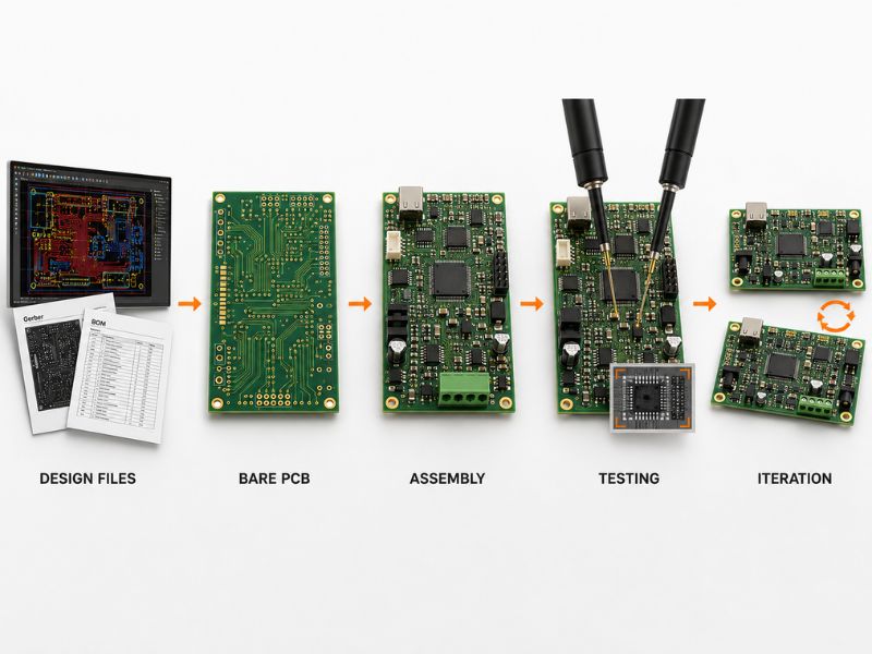
A working PCB prototype turns a schematic into a board you can power on, probe, and validate. The build itself is a short chain — design files, bare-board fabrication, assembly, and test — but small gaps at any step turn into re-spins that cost weeks. The steps below move through that chain and flag the checks that keep a prototype on schedule.
What Is PCB Prototype Manufacturing?
A PCB prototype is a low-volume build used to verify that a design works electrically, fits mechanically, and can be assembled. It is not a cost-optimized product. The goal is fast, accurate validation before committing to volume.
Prototype vs Production: Scope and Goals
Prototype and production runs serve different masters.
| Dimension | Prototype | Production |
| Volume | Low (5–25 pcs typical) | High |
| Priority | Speed and validation | Cost and yield |
| Component sourcing | Flexible, often with alternates | Optimized, locked BOM |
| Test depth | Functional, debug-focused | ICT / FCT, statistical |
Designing a prototype to hit production cost targets usually slows the one thing it should do fastest: prove the concept.
Why a Structured Prototype Process Pays Off
Catching a design error at the file stage costs a DFM review. Catching it after assembly costs a full re-spin plus the lost board time. A defined flow keeps responsibility clear: the designer owns the files, the fabricator owns the bare board, the assembler owns placement and reflow, and test confirms the result.
The structured path also shortens communication. When each stage has a clear input and output, questions route to the right owner instead of bouncing between engineering and the shop floor.
Step 1 — Design and File Preparation
Files You Must Submit
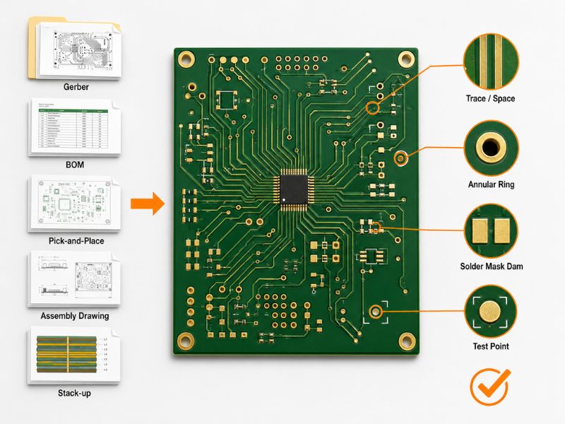
A complete package prevents the most common delay: a fab or assembler waiting on a missing file.
- Gerber (RS-274X or X2) for each layer, plus drill and rout files
- BOM with manufacturer part numbers, quantities, and reference designators
- Pick-and-Place (CPL/XY) file for automated assembly
- Assembly drawing or notes covering orientation, polarity, and any special handling
- Stack-up and impedance notes when controlled impedance is required
- IPC netlist when available, to support electrical test
Missing the CPL or assembly notes is the fastest way to stall a prototype that is otherwise ready to run.
Run a DFM Check Before You Fabricate
DFM (design for manufacturing), DFA (assembly), and DFT (test) reviews catch violations that a board house would otherwise flag mid-build. Common checks:
- Annular ring meets the class requirement (Class 3 outer layer ≥ 2 mil)
- Trace and space within the fabricator’s limit
- Hole size supports the aspect ratio after plating
- Solder-mask dams exist between fine-pitch pads
- Test points are accessible and large enough for probes
RapidDirect runs a free built-in DFM analysis on every order, and prototype boards can start from a 12-hour turn with no minimum quantity. A DFM pass before release is cheaper than a rejected panel.
Step 2 — PCB Fabrication (Bare Board Build)
How the Bare Board Is Built
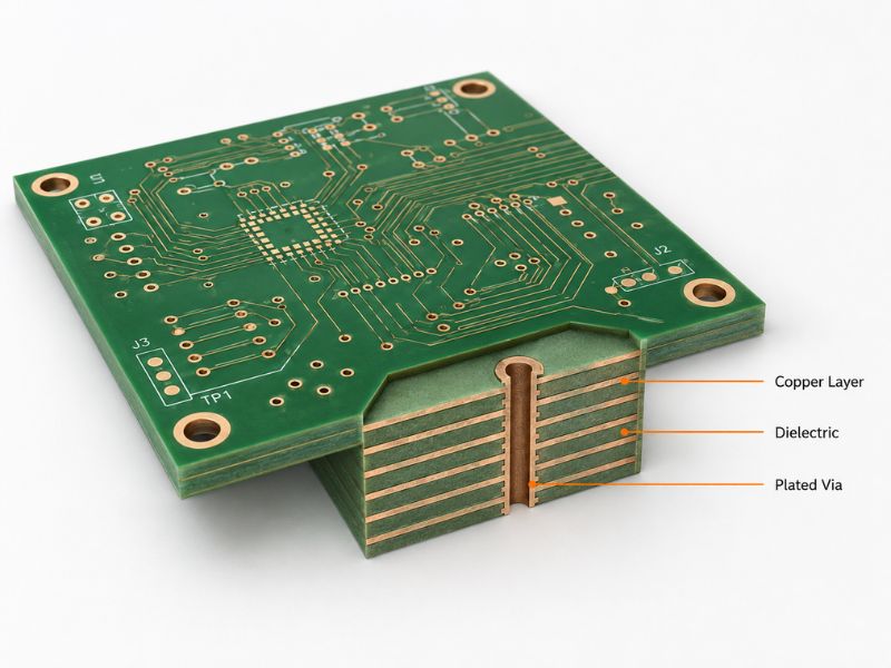
The bare board goes through a set sequence regardless of layer count:
- Inner-layer imaging and etch
- Lamination for multilayer stacks
- Drilling (CNC or laser for microvias)
- Desmear and copper plating
- Outer-layer imaging and etch
- Solder mask and silkscreen
- Surface finish
- Routing and 100% electrical test
Each step has a tolerance budget. Tight impedance or fine line/space should be stated up front, not discovered during test.
Choosing a Surface Finish
Surface finish affects solderability, shelf life, and flatness for fine-pitch parts.
| Finish | Key trait | Best for |
| HASL / Lead-Free HASL | Low cost, robust | General prototypes, through-hole |
| ENIG | Flat Ni/Au, wire-bondable | BGA, fine pitch, aluminum wedge bond |
| OSP | Flat, low cost, Cu-protect | Fine pitch; shorter shelf life |
| Immersion Silver | Flat, excellent solderability | RF/HF, fine pitch; tarnish-sensitive |
| ENEPIG | Ni/Pd/Au, no black-pad | Wire bonding + SMT mixed |
RapidDirect supports HASL, lead-free HASL, ENIG, OSP, immersion silver, and ENEPIG across rigid, HDI, flex, rigid-flex, and metal-core boards.
Step 3 — PCB Assembly
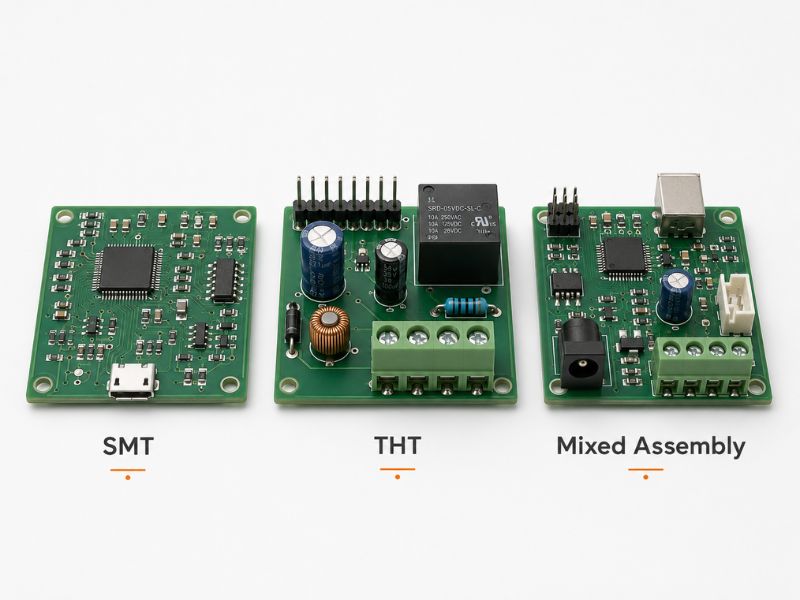
SMT, THT, and Mixed Assembly
Surface-mount technology places most components. Through-hole (THT) handles connectors, large inductors, and mechanical parts that need board strength. Mixed assemblies are the norm for prototypes that bridge digital and power sections.
Component size drives machine capability. Placement down to 01005 passives and BGA pitch down to 0.30 mm is standard on modern lines; confirm the limit before submitting a dense layout.
Turnkey vs Consigned Components
Turnkey assembly puts BOM sourcing on the supplier: authentic parts, alternate suggestions, and managed lead time. Consigned means you ship the parts and the shop mounts them. Partial turnkey splits the two — you keep critical or allocated parts, the supplier sources the rest.
Turnkey suits most prototypes because it removes a sourcing step and keeps one owner for the build. Consigned makes sense when parts are allocated, export-controlled, or already on hand.
Step 4 — Testing and Validation
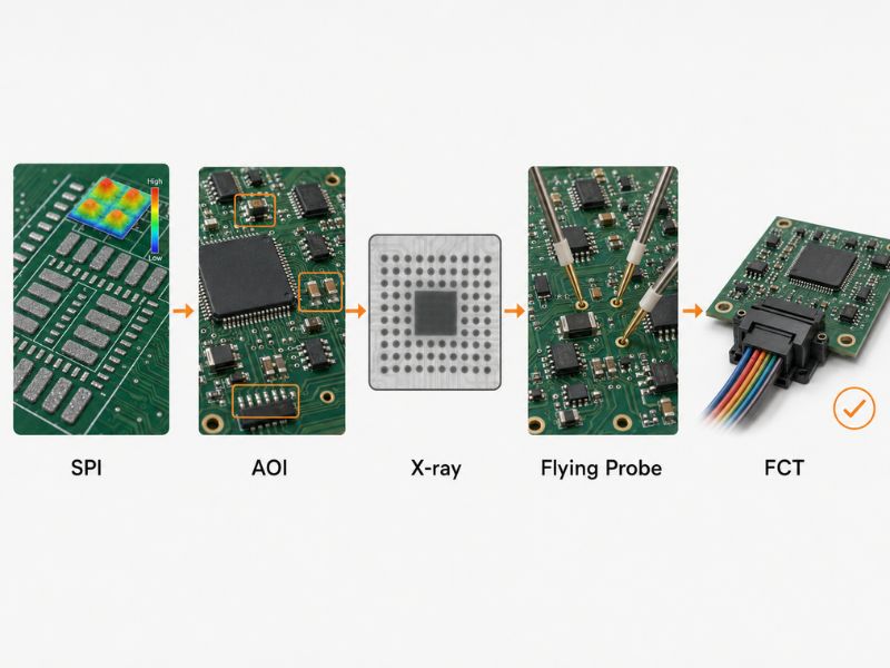
The Prototype Test Chain
Test depth scales with risk, not volume. A typical prototype chain:
- SPI verifies solder-paste volume, placement, and polarity
- AOI catches placement and surface defects
- X-ray inspects hidden joints under BGA and QFN
- Flying probe checks open, short, and continuity
- FCT validates function against the test spec
RapidDirect’s line covers SPI, AOI, X-ray, flying probe, and functional test, with first-article and incoming inspection at the front end.
Flying Probe vs Test Fixture
| Method | Setup | Speed | Best use |
| Flying probe | No fixture, low NRE | Slower per board | Prototypes, low volume, design changes |
| Test fixture (ICT) | Fixture NRE | Fast cycle | Mature design, high volume |
For 5–20 prototype pieces, flying probe avoids fixture cost and adapts when the netlist changes between spins.
How Many Prototypes to Build
Functional validation usually needs 5–20 pieces. The count depends on the test matrix: separate units for burn-in, environmental sampling, and destructive analysis, plus spares for rework practice. Building too few starves parallel tests; building too many wastes setup effort on an unproven design.
Step 5 — Debug, Iterate, and Transition to Production
The first powered board rarely passes every test. Debug, fix the schematic or layout, and re-run. Each spin should close specific open items, not reopen the whole design.
From Prototype to EVT: Planning the Handoff
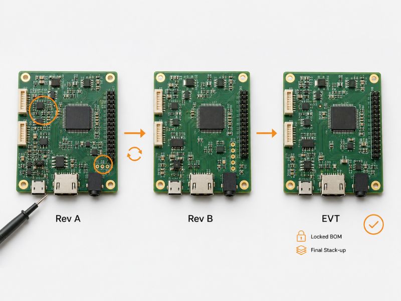
A functional prototype proves the concept. An EVT (Engineering Validation Test) build proves it on production-representative hardware. The sizes below are typical industry practice for validation builds, not a vendor specification — adjust them to your own test matrix:
- Functional prototype: 5–20 pcs, flexible materials and alternates
- EVT: 5–25 pcs built with the final stack-up, material, surface finish, and locked BOM
Plan for 2–3 design iterations between first prototype and EVT. More than that usually signals weak upfront specification rather than a hard technical problem. EVT is the bridge to DVT and volume — treat it as the first build that must survive the real process window.
Common PCB Prototyping Mistakes to Avoid
- Incomplete BOM with no manufacturer numbers or alternate sources
- Missing assembly notes, especially polarity and connector orientation
- No test points or poor DFT, forcing manual probing under a scope
- Optimizing cost over speed at prototype stage, delaying validation
- Late compliance planning — medical, automotive, and industrial boards need EMC and environmental test strategy set early, not after the first build
PCB Prototype DFM Checklist
Run this before releasing files:
- Annular ring meets class (outer ≥ 2 mil at Class 3)
- Trace/space within fab limit (≥ 2/2 mil for fine designs)
- Hole size supports aspect ratio (≥ 0.15 mm CNC, 0.10 mm laser)
- Solder-mask dam present between fine-pitch pads
- Test points ≥ 0.3 mm and probe-accessible
- BGA pitch ≥ 0.30 mm; via-in-pad filled and capped
- Copper weight in range (1/3–13 oz)
- Stack-up documented; impedance notes attached
- Silkscreen clear of pads and test points
- BOM complete with manufacturer P/N and alternates
Conclusion
A PCB prototype moves through five stages — file preparation, bare-board fabrication, assembly, test, and iteration — and the cheap fixes all sit at the front. Submit a complete package, clear a DFM check, pick the surface finish for the parts you actually use, and test with the chain your risk needs.
RapidDirect builds prototype PCBs from a 12-hour turn with no MOQ, runs a free DFM review on every order, and assembles prototypes in 3–5 business days across six SMT lines with a full SPI/AOI/X-ray/flying-probe/FCT chain under ISO 9001, IATF 16949, ISO 13485, and IPC Class 2/3 compliance.
Get an instant quote for your PCB prototype and upload the Gerbers — the DFM feedback comes back with the price.
FAQ
Bare-board prototypes can start from a 12-hour turn with no minimum order at RapidDirect. Assembled prototypes (PCBA) typically run 3–5 business days, with urgent options at 1–2 days when the line and parts allow.
Prototype runs carry setup, engineering, and flexible sourcing costs spread over a few pieces instead of thousands. The premium buys speed and the freedom to change the design. It is worth it whenever a late discovery would force a volume re-spin.
Use turnkey when the BOM is standard and you want one owner for the build. Use consigned or partial turnkey when parts are allocated, export-controlled, or already in stock. Turnkey also gives you alternate-part suggestions you may not have sourced yourself.
Medical programs should look for ISO 13485; automotive needs IATF 16949. Both sit on top of ISO 9001, and IPC Class 3 compliance matters when the board must meet higher reliability. Confirm the certs before the EVT build, not at volume.
Move to EVT once the schematic and layout are stable and you are validating the final material, stack-up, finish, and BOM under the real process. If you are still swapping parts weekly, stay at functional prototype and burn fewer production-grade pieces.
Confirm the locked BOM and alternates, the test coverage (ICT/FCT scope), the inspection records from EVT, and the process capability (Cpk) for critical features. Those items decide whether the handoff to volume is a formality or a new risk round.