
For hardware teams, the printed circuit board is the first thing that gets made and the last thing they want to overpay for. Yet PCB quotes from different suppliers can vary by 50 percent or more for what looks like the same board. The gap is rarely a pricing mistake — it is almost always a difference in the specifications, stack-up decisions, and manufacturing rules embedded in the design files.
Understanding PCB fabrication cost means understanding the variables that fabricators actually price: board size, layer count, material grade, copper weight, minimum trace and hole features, surface finish, panel utilization, quantity, and lead time. This guide breaks down each factor and shows you exactly where the money goes — and where it can be saved.
What Drives PCB Fabrication Cost?
A PCB fab shop quotes each board as a manufacturing process, not a commodity. The price reflects how many process steps the board requires, how much material it consumes, how much setup and tooling it needs, and how likely it is to yield. Boards that follow the fabricator's standard capabilities run through the line efficiently and cost little; boards that push limits — finer traces, exotic materials, blind and buried vias — consume engineering time and yield margin, and they are priced accordingly.
The good news is that most cost drivers are controllable at the design stage. A handful of disciplined choices in the schematic and layout phase can cut fabrication cost by 30 to 50 percent without changing the design's function.
Board Size and Layer Count
Board size matters twice: once for material, once for panelization. Fabricators build boards on standard panels — typically 18×24 inches — and price per square inch of panel used. Smaller boards are cheaper per unit only up to a point, because a fixed amount of panel area is consumed by borders, fiducials, and tooling rails.
Layer count is the single biggest structural cost driver. A 2-layer board is the baseline; every additional pair of layers adds lamination cycles, drilling passes, plating steps, and inspection. Moving from 2 to 4 layers typically increases fabrication cost by 50–80 percent, and 6-layer and 8-layer boards climb steeply from there. Use the minimum layer count that supports your routing and signal-integrity needs.
Material Selection
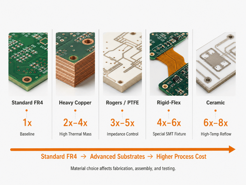
Standard FR-4 is the default for good reason: it is cheap, capable, and available everywhere. Cost climbs when the application demands high-frequency laminates such as Rogers or PTFE-based materials, high-Tg FR-4 for lead-free assembly and thermal stress, or aluminum-backed boards for LED and power applications. If you are weighing exotic laminates against standard grades, compare the properties and cost trade-offs of the options in our materials guide before committing the stack-up.
Material thickness and copper weight also influence cost. Standard 1.6 mm boards with 1 oz copper are the most economical; non-standard thicknesses and heavy copper (3 oz and up) slow the etch and drilling process. When a design truly needs specialty laminates, minimize the number of layers on them — hybrid stack-ups put the expensive material only where the RF or thermal requirement exists.
Copper Weight and Minimum Features
Minimum trace width and spacing, minimum hole size, and hole aspect ratio determine whether a board runs on standard equipment. Common economical baselines are 6/6 mil trace/space, 0.3 mm minimum finished hole, and a 10:1 hole aspect ratio. Designs that push below these numbers require finer imaging, more expensive drills, or laser drilling — all of which raise PCB fabrication cost.
Hole count is another overlooked variable. Each drilled hole is a discrete operation, and thousands of vias add real machine time. In non-critical areas, larger pads and fewer, larger vias keep the board cheaper without hurting performance.
Surface Finish Options
Surface finish protects exposed copper and ensures solderability. The finish is selected for the assembly process and the product environment — but each option carries a different price:
- HASL (hot air solder leveling) is the lowest-cost finish and perfectly adequate for most through-hole and general SMT boards.
- OSP (organic solderability preservative) is inexpensive and flat, ideal for fine-pitch SMT, though it has a shorter shelf life.
- ENIG (electroless nickel immersion gold) costs more but gives a flat, corrosion-resistant, wire-bondable surface with long shelf life — the standard for higher-reliability products.
- Immersion silver and immersion tin sit between OSP and ENIG in price, chosen for specific assembly and environmental needs.
Choosing the finish to match the assembly process — rather than defaulting to the most expensive option — is one of the easiest cost optimizations available.
Quantity, Panelization, and Lead Time
Quantity drives cost through fixed-cost amortization. Tooling, engineering review, and setup are the same whether you order 5 boards or 500. Small batches therefore carry a high per-board price; costs per board fall sharply as volume rises and the fixed overhead spreads across more units.
Panelization is the lever that multiplies your board area efficiently. A well-designed panel with high utilization — multiple boards, rails, and tooling holes arranged to use nearly all the panel — directly lowers per-unit cost. Standard-size boards that panel cleanly are cheaper than odd-sized boards that leave dead area.
Lead time is a multiplier: standard 5–7 day turns are the baseline, and expedited turns of 24–72 hours carry significant premiums. Planning ahead is, quite literally, money in the bank. And when your product also needs precision-machined metal enclosures, heat sinks, or connector housings, sourcing the boards and the CNC machined parts from partners who coordinate well keeps the whole program on schedule.
How to Reduce PCB Fabrication Cost
These design and sourcing practices consistently deliver the biggest savings:
- Consolidate to the minimum layer count that meets your electrical requirements.
- Stay within standard capabilities: 6/6 mil trace/space, 0.3 mm holes, standard 1.6 mm board thickness.
- Use standard FR-4 and 1 oz copper unless the design truly demands more.
- Match the surface finish to the assembly process instead of over-specifying.
- Design for panel efficiency — standard sizes, sensible board-to-board spacing, and shared rails.
- Order realistic quantities for your stage: prototypes in small batches, production in volumes that amortize setup.
- Request DFM feedback before ordering — a good fabricator will flag features that push cost without adding value. For boards destined for critical or regulated products, review the inspection and documentation practices of your partners against our quality assurance process to make sure your supply chain meets the bar.
Frequently Asked Questions
How much does PCB fabrication cost per board?
A simple 2-layer prototype board typically costs a few dollars per board at small quantities, while complex multilayer or high-frequency boards can cost ten to a hundred times more. Total cost depends on size, layers, material, features, quantity, and lead time — there is no single per-board price.
Why is my PCB quote so much higher than expected?
The most common culprits are non-standard layer counts, fine trace/space below 6/6 mil, small or odd-sized boards that panel poorly, expensive surface finishes, and expedited lead times. Compare your design against the fabricator's standard capabilities to find the cost drivers.
Does PCB size affect cost?
Yes, but not linearly. Material cost scales with area, while panel utilization determines how many boards fit on a standard panel. A board sized to panel efficiently will cost less per unit than an odd-sized board that wastes panel area.
What is the cheapest PCB surface finish?
HASL is generally the lowest-cost finish and works well for most through-hole and standard SMT assemblies. OSP is also inexpensive and flat for fine-pitch parts. ENIG costs more but is justified for high-reliability, long-shelf-life, or wire-bonding applications.
How can I reduce my PCB fabrication cost?
Use the minimum layer count, stick to standard materials and features, match the surface finish to assembly, design for panel efficiency, order realistic quantities, and plan lead times instead of paying for expedites.
Get a Cost-Effective PCB Quote
Whether you are validating a prototype or ramping to production, the fastest way to control PCB fabrication cost is to pair your layout with experienced manufacturing input. At SHBD Metal, our engineering team reviews your design files, flags cost drivers before you commit, and works with trusted fabrication partners to deliver boards that meet your spec without waste.
Upload your Gerber files and design documents today and receive a detailed quote within hours. We are ready to help you build it smarter.