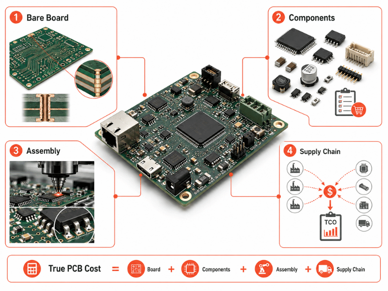
In hardware development, predicting the total cost of a printed circuit board (PCB) assembly often feels like navigating a maze of hidden fees. When budgeting for an upcoming electronics project, hardware engineers and NPI sourcing managers frequently ask, “how much does a PCB cost?” The reality is that the true custom PCB board cost is never a single, static number. It is a dynamic calculation composed of bare board fabrication, global component sourcing, and final assembly complexities.
More importantly, relying on a fragmented supply chain—where you source boards from one vendor, buy components from a broker, and machine enclosures at a third-party shop—is the fastest way to inflate your project’s Total Cost of Ownership (TCO). This guide breaks down the core elements of PCB pricing and demonstrates how partnering with an integrated, end-to-end ODM/NPI manufacturer reduces your budget while guaranteeing international compliance.
5 Key Factors That Determine the Cost of PCB Board Fabrication
The physical fabrication of the bare board is the foundation of your PCB cost. Understanding the engineering tolerances that drive up production expenses allows you to design for manufacturability (DFM) and keep budgets under control.
PCB Cost Drivers Matrix
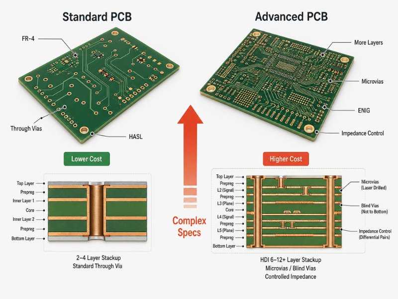
| Cost Factor | Impact on Price | Cost Reduction Tip |
| Layer Count & Size | High | Consolidate routing to reduce layers (e.g., from 6 to 4) and minimize overall board dimensions to increase panel yield. |
| Base Material | Medium to High | Stick to standard FR-4 for general electronics; only specify High-TG, Halogen-Free, or Polyimide when thermal/frequency needs dictate. |
| Via Technology | High | Use standard through-hole vias whenever possible; blind, buried, and micro-vias require multiple lamination cycles, drastically increasing costs. |
| Surface Finish | Medium | HASL (Lead-Free) is the most cost-effective; reserve ENIG or Immersion Silver for fine-pitch BGA or high-reliability requirements. |
| Impedance Control | Medium | Only specify impedance control on critical high-frequency traces; applying it globally requires strict dielectric testing and raises costs. |
Layer Count and Board Size
The physical dimensions of your design and the number of layers directly dictate the amount of raw material (fiberglass and copper foil) consumed. A standard 2-layer board is highly economical, while progressing to 4, 8, or advanced 60-layer HDI structures introduces exponential complexity. Each additional layer requires more alignment precision, lamination pressing time, and inspection, directly increasing the cost of pcb board fabrication.
Base Materials (FR4 vs. Advanced Substrates)
Standard FR-4 material is highly cost-effective and suitable for the vast majority of consumer electronics. However, if your design operates in extreme thermal environments or handles high-frequency RF signals, you must upgrade to specialized substrates like High-TG FR-4, PTFE, Polyimide (for rigid-flex), or Metal Core options (Aluminum/Copper Core). These advanced base materials carry a significant premium over standard FR-4.
Surface Finishes
The surface finish protects exposed copper from oxidation and provides a solderable surface for assembly. Lead-Free HASL (Hot Air Solder Leveling) is the industry standard for budget-conscious projects. However, if your design features tight-pitch components like BGAs, the uneven surface of HASL will cause soldering defects. In these cases, upgrading to ENIG (Electroless Nickel Immersion Gold) or OSP is mandatory to ensure flat pads, though it increases the initial pcb pricing.
Vias and Drilling Complexity
Every hole drilled into a PCB incurs machine time and tool wear. While standard mechanically drilled through-hole vias are inexpensive, advanced HDI (High-Density Interconnect) designs require laser-drilled micro-vias, blind vias, or buried vias. These advanced via structures require the board to undergo multiple pressing and drilling cycles, which can easily double the fabrication cost.
PCB Assembly & Component Sourcing: The Hidden Cost Drivers
The bare board is only a fraction of the total custom pcb board cost. The true financial variables lie in how you procure the silicon and attach it to the board.
Turnkey Sourcing vs. Consigned Sourcing
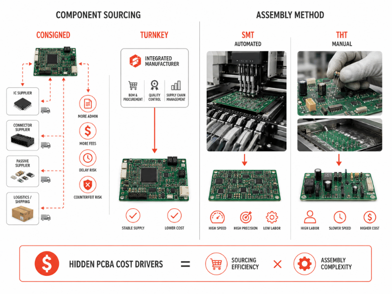
Attempting to source components internally (Consigned) often leads to administrative bloat, excessive shipping fees, and the risk of purchasing counterfeit parts on the gray market. Utilizing a Turnkey service—where the manufacturer handles the entire BOM (Bill of Materials)—optimizes costs via scaled procurement.
By leveraging a global supply chain layout, a premier manufacturer guarantees 100% authentic parts while providing strict quality control and stable lead times, ultimately lowering your per-unit cost.
SMT vs. THT Assembly
Surface Mount Technology (SMT) is highly automated, allowing pick-and-place machines to populate thousands of components per hour, keeping assembly costs low. Conversely, Through-Hole Technology (THT) often requires manual insertion and wave soldering. Minimizing THT components in your design will significantly reduce manual labor charges and accelerate assembly time.
Prototyping vs. Mass Production Pricing Strategies
Hardware teams must adopt different pricing expectations as a product moves through the NPI lifecycle.
During the Engineering Verification stage, absolute low cost is less important than speed and design validation. Utilizing a professional pcb prototype serviceallows teams to rapidly iterate. While the per-unit cost of a prototype is higher than mass production due to setup amortization, it prevents catastrophic errors in the final build.
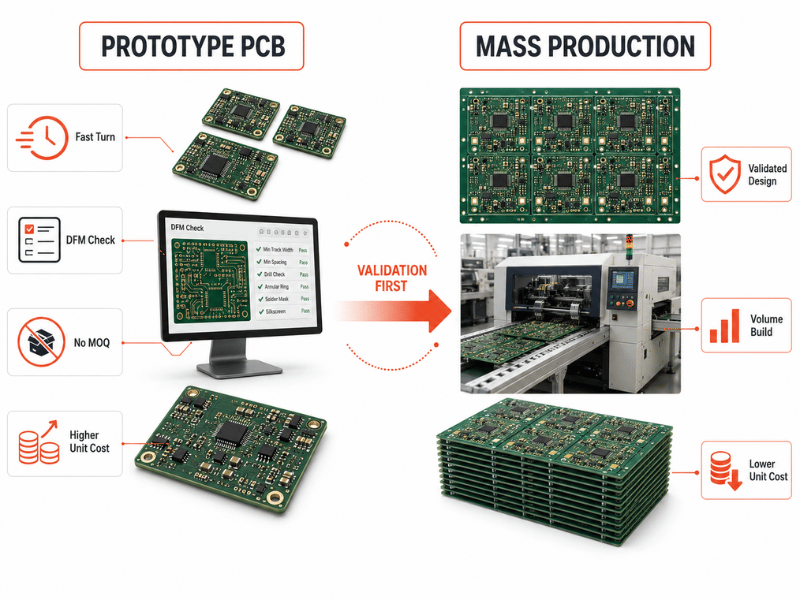
For agile hardware teams, speed is critical. Advanced facilities can deliver prototype PCBs in as fast as 12 hours with no Minimum Order Quantity (MOQ). Furthermore, built-in, hassle-free DFM (Design for Manufacturability) analysis during the quoting phase ensures that layout flaws are corrected before a single board is etched, saving thousands of dollars in potential rework.
Accelerating NPI: The Value of an Integrated Manufacturing Partner
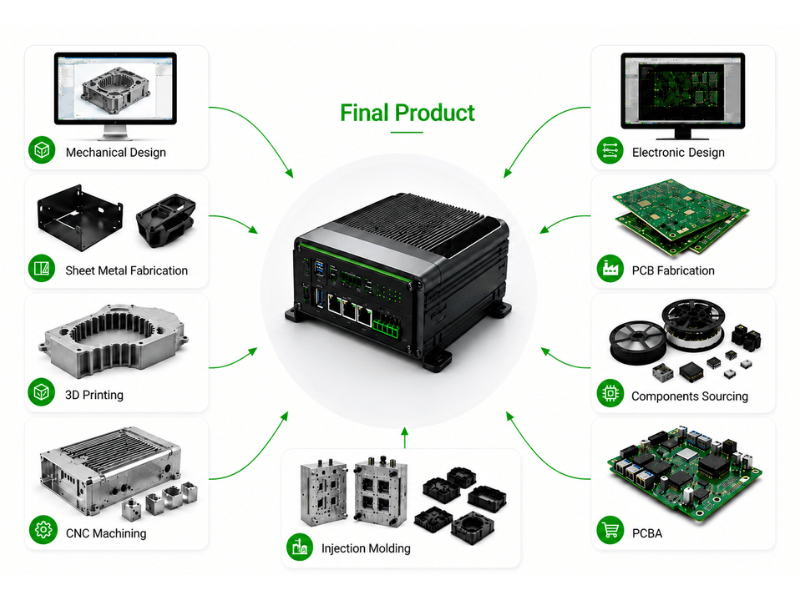
The most significant way to optimize your pcb pricing is to stop treating electronic and mechanical manufacturing as isolated silos. Moving a product into production efficiently requires a connected product development journey.
By integrating PCB design, bare board manufacturing, PCBA component sourcing, and mechanical parts fabrication (CNC Machining, 3D Printing, Injection Molding, and Sheet Metal) under one roof, you eliminate the friction of managing multiple vendors. This End-to-End ODM/NPI support accelerates prototype development and ensures production readiness. Our AI-powered platform enables instant quoting and real-time order visibility, turning product ideas into working prototypes seamlessly from BOM to tested board.
Quality and Compliance as a Cost Saver
Recalls and field failures are the most expensive costs in manufacturing. Ensuring your PCB assembly meets strict international standards is a non-negotiable financial safeguard. Facilities operating under IPC Class 2/3 compliance and holding key certifications—including ISO 9001 (Quality Management), IATF 16949 (Automotive), ISO 13485 (Medical Devices), and ISO 14001 (Environmental)—ensure that your products are built to the highest global standards, mitigating risk and protecting your bottom line.
Ready to eliminate hidden costs and accelerate your NPI timeline? Stop waiting days for fragmented supply chain estimates. Upload your Gerber files and BOM to our intelligent platform today. Our system will instantly generate a transparent, itemized quote, while our manufacturing experts provide a complimentary DFM analysis to catch costly design flaws before production begins. Streamline your entire hardware journey—from bare board fabrication to final mechanical enclosure assembly—and secure your production schedule now.
FAQ About PCB Pricing
The most effective way to reduce costs is to utilize standard manufacturing specifications (e.g., standard FR-4, 1.6mm thickness, standard copper weight) and minimize layer counts. Additionally, avoid advanced features like blind/buried vias unless absolutely necessary. Most importantly, take advantage of our free built-in DFM analysis to identify and eliminate cost-driving design flaws before production begins.
Expedited manufacturing requires a factory to prioritize your job, disrupt standard scheduling, and dedicate exclusive machine time and labor to your panels. While a 12-hour turn carries a premium, our intelligent, AI-powered platform and advanced facilities optimize routing to deliver fast turnarounds without excessive overhead, keeping emergency NPI projects on track.
Rarely. While it may seem cheaper on a spreadsheet, sourcing your own components introduces severe logistical risks. Delays in receiving a single microchip can halt an entire assembly line. By utilizing our global component sourcing service, you benefit from our scaled purchasing power, strict quality control, and 100% authentic part guarantee, ultimately lowering the total cost of ownership and ensuring stable lead times.