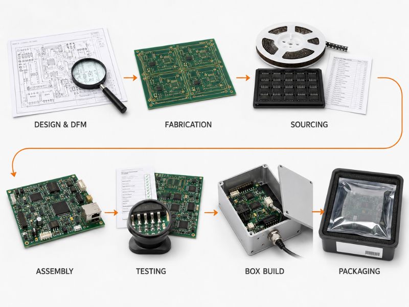
A PCB moves through a fixed sequence before it becomes a working device: design and DFM review, bare-board fabrication, component sourcing, assembly, test, and final integration. Each stage has its own failure modes and lead-time drivers. Understanding where time is spent — and where an integrated manufacturer can compress it — is what separates a project that ships on schedule from one that slips at the box-build step.
This guide walks the full PCB manufacturing process end-to-end. It also shows where quick-turn prototyping and integrated EMS sourcing create real leverage, so you can scope a build that actually hits your dates.
What Is the PCB Manufacturing Process?
The PCB manufacturing process is the chain of operations that turns a schematic into a populated, tested device. In an electronic manufacturing service (EMS) model, one partner owns most or all of these steps:
- Design and DFM review — the schematic and layout are checked for manufacturability before anything is built.
- Bare-board fabrication — copper, dielectric, and solder mask become the physical printed circuit board.
- Component sourcing — the BOM is procured, with authenticity and lead-time checks.
- PCB assembly (PCBA) — parts are placed and soldered onto the board.
- Testing and quality assurance — electrical and functional checks verify the build.
- Box build and integration — the board joins its enclosure, cabling, and mechanical parts.
- Packaging and shipping — outgoing quality control and custom packaging prepare the unit for delivery.
The same seven stages apply whether you need five prototype boards or fifty thousand production units. What changes is how much of the chain a single partner controls, and how tightly the handoffs between stages are managed.
Step 1: PCB Design and DFM Review
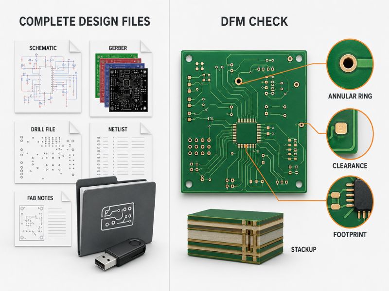
Everything starts with the design files: schematic, netlist, Gerbers, drill files, and fabrication notes. The first real gate is design for manufacturability (DFM) review.
A DFM check catches issues that pass electrical simulation but fail on the floor — insufficient annular rings, non-standard clearances, footprint mismatches, and stackups that cannot be reliably laminated. Catching these before fabrication avoids a scrapped panel and a restarted clock.
This stage is also where prototype iteration begins. Each design revision needs a new board, so the speed of the DFM loop sets the pace for the whole development program. RapidDirect runs free built-in DFM analysis on every order, so the first review happens without a separate charge or a separate submission step.
Step 2: PCB Fabrication — Building the Bare Board
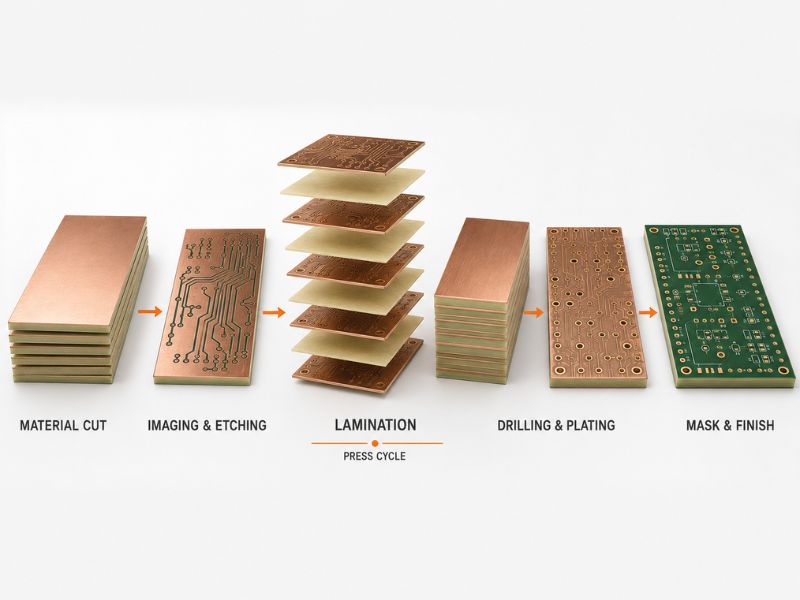
Fabrication turns design data into a physical board through a sequence of material and chemistry steps:
- Material selection and cut. Base laminate (typically FR4, or a specialty substrate for RF, flex, or metal-core builds) is cut to panel size.
- Inner-layer imaging and etching. Copper is patterned into traces on each inner layer.
- Lamination. Inner layers are pressed with prepreg into a multilayer stack. Every layer pair adds a press cycle that cannot be skipped.
- Drilling and plating. Holes and vias are drilled, then plated to establish electrical connection between layers.
- Outer-layer imaging and etching. The outer copper is patterned.
- Solder mask and silkscreen. The protective mask and component markings are applied.
- Surface finish. HASL, ENIG, OSP, or another finish prepares pads for soldering.
The hard lead-time constraint is the lamination press cycle. A 2-layer board can ship in days; an 8-layer board needs multiple press cycles regardless of how much expedite premium you pay. For prototype work, fabrication can run as fast as 12 hours with no minimum order quantity when the design stays within standard material specs.
Step 3: Component Sourcing
Assembly cannot start until the BOM is in hand. Sourcing covers far more than clicking “add to cart”:
- Authenticity verification. Counterfeit or recycled parts create field failures that no amount of test catches upfront.
- Lead-time and allocation checks. Allocated, end-of-life, and hard-to-find parts can stall a build for weeks.
- Alternative part suggestions. A BOM review can flag a single-sourced component and propose a cross-referenced substitute before it becomes a shortage.
Global sourcing with 100% authentic-part guarantee, multi-channel price comparison, and shortage or obsolete-part support matters most on prototype and low-volume runs, where a single missing line item blocks the entire order.
Step 4: PCB Assembly — SMT and Through-Hole
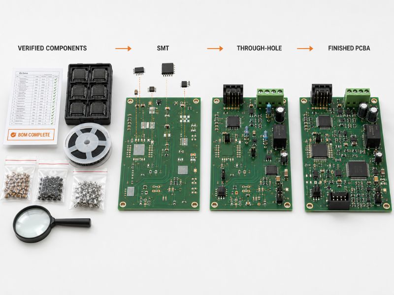
Assembly populates the bare board. The dominant process is surface-mount technology (SMT):
- Solder paste application via stencil, verified by solder-paste inspection (SPI).
- Component placement by pick-and-place machines, down to 01005 passives and fine-pitch BGAs.
- Reflow soldering, where the paste melts and forms joints.
- Through-hole insertion for connectors, transformers, and large parts, finished by wave or selective soldering.
Mixed SMT and through-hole builds are common, and inspection runs inline: AOI catches placement and polarity errors, X-ray inspects hidden BGA and QFN joints. Turnkey assembly — where the manufacturer sources parts and populates on one expedited timeline — typically runs 3–5 business days for prototypes and 1–2 business days for urgent orders.
Step 5: Testing and Quality Assurance
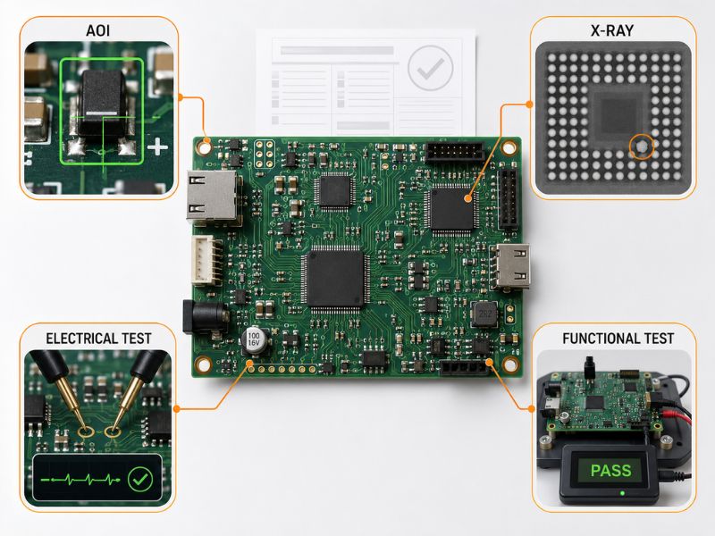
Test is where a board proves it works, not just that it was built. A typical QA flow layers several checks:
- Flying-probe or in-circuit test (ICT) for open, short, and continuity faults.
- X-ray and AOI for joint integrity on hidden and fine-pitch packages.
- Functional testing against the product’s actual operating requirements.
- First-article inspection (FAI) and incoming-quality control (IQC) at defined gates.
The value of test scales with volume. On a five-board prototype, one bad joint is easy to find by hand; on a 50,000-unit run, only a structured test plan keeps escape rate acceptable.
Step 6: Box Build and Final Integration
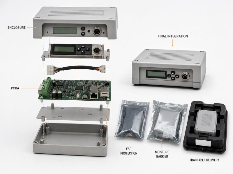
Many devices are not a bare board in a static bag — they are a board inside an enclosure with cabling, displays, and mechanical parts. Box build integrates the PCBA with:
- Enclosures and structural parts (CNC, sheet metal, or molded).
- Wire harnesses, connectors, and sub-assemblies.
- Firmware loading and final configuration where required.
This stage is where electronics and mechanical work meet. A partner with in-house mechanical services can develop the enclosure alongside the PCBA, which removes a cross-supplier handoff and keeps tolerances consistent between the board and its housing.
Step 7: Packaging, OQC, and Shipping
The final stage is outgoing quality control, custom packaging, and shipment. Packaging is not cosmetic: ESD protection, moisture barriers for moisture-sensitive parts, and labeled kitting directly affect field reliability and rework rate on arrival. For medical, automotive, and industrial programs, traceability documentation at this stage supports downstream compliance and recall management.
Where Quick Turn and Prototyping Fit in the Process
Quick turn is not a separate process — it is the same seven stages run on a compressed clock. The leverage shows up at three points:
| Process Stage | What “quick turn / prototype” means here | Accelerated option |
|---|---|---|
| Design & DFM | Iterate fast on every revision | Free built-in DFM on every order |
| Fabrication | Prototype boards in days, not weeks | Bare-board prototypes as fast as 12 hours, no MOQ |
| Assembly | Populated boards on the same expedited timeline | Turnkey PCBA prototypes 3–5 business days (urgent: 1–2) |
The tradeoff is the same as any expedite: less time to catch errors. Clean, verified files and a fast DFM loop matter more here than on a standard run. For the full lead-time tiers and cost premiums across same-day through 5-day turns, see the quick turn PCB guide.
How to Choose an EMS Partner for the Full Process
When the project needs more than a bare board, the partner question becomes whether one supplier can own the chain. Evaluate on concrete factors:
- Integrated capability. Does the partner cover fabrication, sourcing, assembly, test, and box build, or will you stitch several suppliers together?
- DFM speed and depth. A rapid, substantive DFM review — not a file-format check — protects the schedule on every stage.
- Sourcing depth. Global authentic sourcing, BOM review with alternative suggestions, and support for allocated or obsolete parts keeps the line running.
- Quality at scale. Ask for first-pass yield and on-time delivery on expedited and volume runs specifically, not company-wide averages.
- Communication. A DFM hold, material shortage, or test failure must reach you immediately, not after the deadline passes.
RapidDirect operates as a full EMS. Every order includes free DFM, prototype fabrication as fast as 12 hours with no MOQ, and turnkey PCBA in 3–5 business days (urgent: 1–2). Component sourcing is global and authentic, with shortage and end-of-life support. The operation holds ISO 9001, IATF 16949 (automotive), and ISO 13485 (medical) certifications with IPC Class 2/3 compliance, runs 6 SMT lines in a 30,000 sqm smart factory, and supports box build and enclosure development alongside the PCBA.
Conclusion
The PCB manufacturing process is the same seven stages regardless of who runs it. The difference is how many of those stages one partner controls, and how tightly the handoffs are managed. Keep designs inside standard material specs, submit complete verified files, and choose a partner on integrated capability and DFM speed — not on the lowest bare-board price alone.
Get an instant quote for your PCB manufacturing project and scope the right process path from design to device.
FAQ
For a prototype, the chain can close in roughly a week when fabrication and assembly both run on expedited timelines — bare boards in as fast as 12 hours and turnkey PCBA in 3–5 business days. Volume production adds sourcing, pilot runs, and process qualification, typically extending to several weeks depending on component lead times and order volume.
Yes. Internal checks confirm the circuit works; DFM confirms it can be built reliably. Footprint mismatches, non-standard clearances, and stackups that will not laminate cleanly often pass simulation but fail on the floor. A manufacturer-side DFM loop catches these before fabrication spends material and time.
A prototype run validates the design with low quantity and fast iteration; scrap at the next revision is expected and cheap. Production runs optimize for yield, process control, and consistency across thousands of units, with structured test and traceability. The process steps are the same, but the quality gates and volumes differ.
Use a full EMS when the project needs assembly, component sourcing, test, and box build — not just a bare board. A fabrication-only shop leaves you stitching assembly, sourcing, and integration across separate suppliers, which adds handoffs, communication lag, and traceability gaps.
Yes, when the operation runs global sourcing with allocated, end-of-life, and hard-to-find part support. A BOM review that flags single-sourced or discontinued lines and proposes cross-referenced alternatives prevents a shortage from stalling the build.
Quick turn compresses the same seven stages rather than replacing them. Use it at the design-and-DFM, fabrication, and assembly stages when a revision or deadline is time-critical, and keep standard lead times for steps that do not need speed. The board still meets the same IPC and quality standards — only the clock changes.